In December, Wikichip reported that TSMC's 3nm process showed practically no improvement in density over the company's previous 5nm node with respect to SRAM density. The publication asked one simple question: Did we just witness the death of SRAM? At least in Wikichip's opinion, "historical scaling is officially dead."
This idea has massive ramifications for the entire tech industry, and its effects will be felt in PCs and other devices for years to come. But you may be asking yourself what all this means and whether you should care. In order to understand how the "death of SRAM" will impact PCs and how chip designers will deal with it, we need to talk about nodes, Moore's Law, and cache.
Moore's Law was dying gradually, and now suddenly
Moore's Law is the semiconductor industry's benchmark for success and holds that newer chips should have twice the amount of transistors than chips from two years ago. Intel, AMD, and other chip designers want to make sure they're keeping pace with Moore's Law, and failing to keep up means losing the technological advantage to competitors.

Since processors can only be so large, the only reliable way to increase transistor count is to shrink them and pack them together more densely. A node or process is how a semiconductor manufacturer (also called fabs and foundries) makes a chip; a node is usually defined by the size of a transistor, so the smaller the better. Upgrading to the latest manufacturing process was always a reliable way to increase transistor count and performance, and for decades, the industry has been able to meet all of the expectations.
Unfortunately, Moore's Law has been dying for years now, since around 2010 when the industry hit the 32nm mark. When it tried to go further, it hit a brick wall. Almost every fab from TSMC to Samsung to GlobalFoundries struggled to develop anything smaller than 32nm. Eventually, new technologies were developed that made progress possible once more, but transistors are no longer getting smaller in the same way they used to. The name of a node no longer reflects how small the transistor actually is, and new processes no longer bring the density gains they used to.
The industry hit a brick wall when it tried to go further than the 32nm mark in 2010.
So what's up with TSMC's 3nm node? Well, there are two main types of transistors that are in a typical processor: those for logic and those for SRAM, or cache. Logic has been easier to shrink than cache for a while (cache is already really dense), but this is the first time we've seen a foundry like TSMC fail to shrink it at all in a new node. A variant of 3nm with significantly higher cache density is expected at some point, but TSMC certainly hit an inflection point where scaling is very minor, and other fabs may encounter the same problem.
But the problem isn't just about not being able to increase the amount of cache without using up more area. Processors can only be so large, and any space taken up by cache is space that can't be used for logic, or the transistors that lead to direct performance gains. At the same time, processors with more cores and other features need more cache to avoid memory-related bottlenecks. Even though the density of logic continues to increase with every new node, it might not be enough to compensate for the lack of SRAM scaling. This might be the killing blow for Moore's Law.
How the industry can solve the SRAM problem

There are three goals high-performance processors need to meet: size is limited, cache is required, and new nodes will no longer reduce the size of cache much if at all. While it's possible to increase performance via architectural improvements and higher clock speeds, adding more transistors has always been the easiest and most consistent way to achieve a generational speed boost. In order to overcome this challenge, one of these fundamentals needs to change.
As it turns out, there is already a perfectly working solution to the SRAM problem: chiplets. It's the technology that AMD has been using since 2019 for its desktop and server CPUs. A chiplet design uses multiple pieces of silicon (or dies), and each die has one or just a few functions; some might just have cores for instance. This is in opposition to a monolithic design where everything is in a single die.
Chiplets get around the size issue, and they're a key part as to why AMD has been able to keep up with Moore's Law. Remember, Moore's Law isn't about density, but transistor count. With chiplet technology, AMD has been able to create processors with a total die area of over 1,000 mm2; manufacturing this CPU in just a single die is probably impossible.

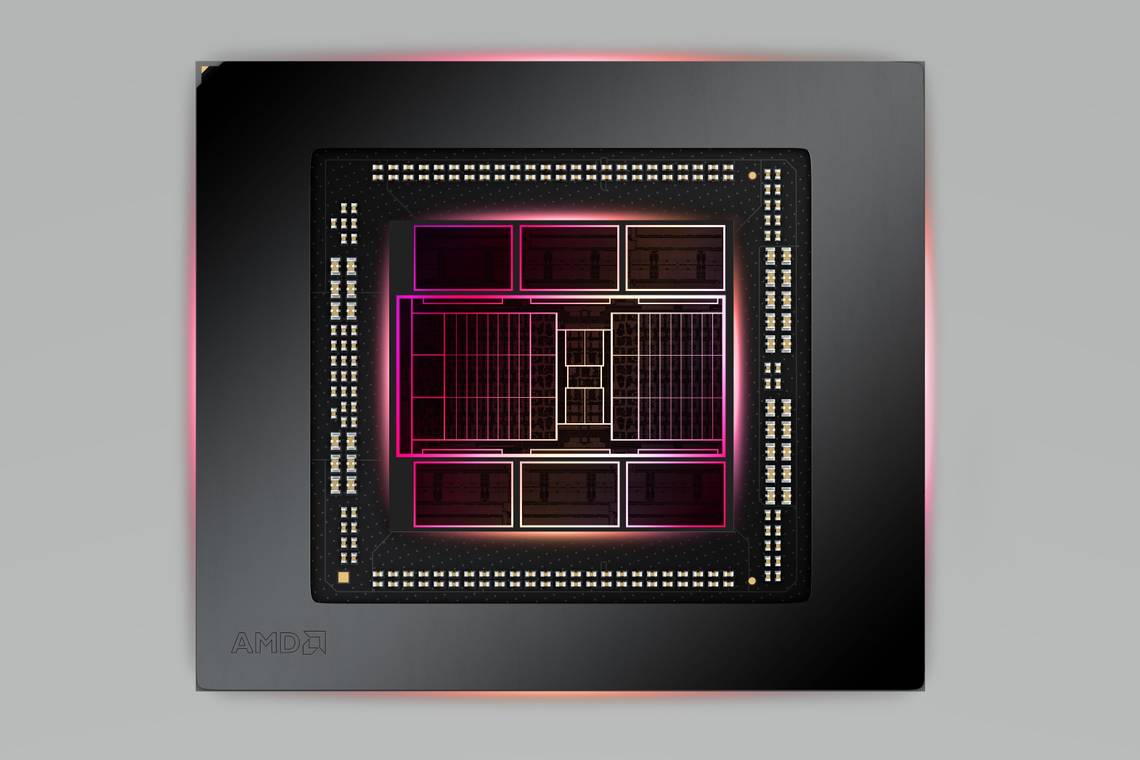
The single most important thing AMD has done that mitigates the cache issue is to put cache on its own die. The V-Cache inside the Ryzen 7 5800X3D and the memory chiplets in the RX 7000 series are an example of cache chiplets in action. It's likely that AMD saw the writing on the wall since cache has been difficult to shrink for years now, and now that cache can be partitioned from everything else, it leaves more space for larger chiplets with more cores. The RX 7900 XTX's main die is only about 300 mm2, which means there's plenty of room for AMD to make a larger die if it wants.
Chiplets aren't the only way, though. Nvidia's CEO recently proclaimed the death of Moore's Law. The company itself relies on its artificial intelligence technology to achieve greater performance without needing to move away from a monolithic design. Its newest Ada architecture is theoretically many times faster than last generation's Ampere thanks to features like DLSS 3. However, we will see in the coming years if Moore's Law must be kept alive or if new technologies can mirror the performance benefits of adding more transistors without actually having to add any.