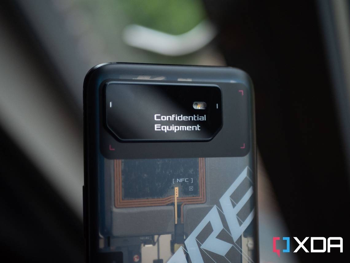
In December 2021 at a launch event in Hawaii, we saw Qualcomm unveil the Snapdragon 8 Gen 1. It packed more performance than ever, and the company also claimed efficiency improvements. However, it wasn't that much more powerful than chipsets of previous years. Now the Snapdragon 8 Plus Gen 1 is here, and ASUS has kindly provided us with an SM8475 Engineering Device to run our own benchmarks on ahead of its release.
We ran multiple benchmarks on the SM8475 Engineering Device that we received from ASUS, including one holistic benchmark (AnTuTu), a CPU-centric benchmark (Geekbench), and a GPU-centric benchmark (GFXBench). As well, we also made use of Burnout Benchmark to measure the power consumption of the chipset, particularly when compared to the Snapdragon 8 Gen 1. The Snapdragon 8 Plus Gen 1 is fabricated by TSMC (the 8 Gen 1 was fabricated by Samsung Foundry) and some believe that it will improve efficiency and heat as a result.
For testing, we enabled ASUS' X-Mode. The reason for this is that the device we received is very much a work in progress. X-Mode is the first feature that the company tunes for chipsets, and as such, will make the most out of the Snapdragon 8 Plus Gen 1. These scores are for reference only, and serve to show the maximum capabilities of this new chipset in prime conditions.

About this article: ASUS supplied us with an SM8475 Engineering Device/Testing Platform for the purposes of assessing the benchmark and gaming performance of the Qualcomm Snapdragon 8 Plus Gen 1. ASUS had no input into the contents of this article.
Benchmarks overview
- AnTuTu: This is a holistic benchmark. AnTuTu tests the CPU, GPU, and memory performance, while including both abstract tests and, as of late, relatable user experience simulations (for example, the subtest which involves scrolling through a ListView). The final score is weighted according to the designer’s considerations.
- GeekBench: A CPU-centric test that uses several computational workloads including encryption, compression (text and images), rendering, physics simulations, computer vision, ray tracing, speech recognition, and convolutional neural network inference on images. The score breakdown gives specific metrics. The final score is weighted according to the designer’s considerations, placing a large emphasis on integer performance (65%), then float performance (30%), and finally cryptography (5%).
-
GFXBench: Aims to simulate video game graphics rendering using the latest APIs. Lots of onscreen effects and high-quality textures. Newer tests use Vulkan while legacy tests use OpenGL ES 3.1. The outputs are frames during test and frames per second (the other number divided by the test length, essentially), instead of a weighted score.
- Aztec Ruins: These tests are the most computationally heavy ones offered by GFXBench. Currently, top mobile chipsets cannot sustain 30 frames per second. Specifically, the test offers really high polygon count geometry, hardware tessellation, high-resolution textures, global illumination and plenty of shadow mapping, copious particle effects, as well as bloom and depth of field effects. Most of these techniques will stress the shader compute capabilities of the processor.
- Manhattan ES 3.0/3.1: This test remains relevant given that modern games have already arrived at its proposed graphical fidelity and implement the same kinds of techniques. It features complex geometry employing multiple render targets, reflections (cubic maps), mesh rendering, many deferred lighting sources, as well as bloom and depth of field in a post-processing pass.
- CPU Throttling Test: This app repeats a simple multithreaded test in C for as short as 15 minutes, though we ran it for 30 minutes. The app charts the score over time so you can see when the phone starts throttling. The score is measured in GIPS -- or billion operations per second.
- Burnout Benchmark: Loads different SoC components with heavy workloads to analyze their power consumption, thermal throttling, and their maximum performance. It uses Android's BatteryManager API to calculate the watts being used during testing, which can be used to understand the battery drain on a smartphone.
In testing the SM8475 Engineering Platform, we put it up against the OnePlus 10 Pro and the RedMagic 7 in their out-of-the-box configurations. This means that the OnePlus 10 Pro has a throttle already placed on the chipset (that we identified in our review), whereas the RedMagic 7 is largely unhindered. The OnePlus 10 Pro is a more popular and relatable configuration, whereas the RedMagic 7 is one of the best performing. The Snapdragon 8 Gen 1 was tamed through software in different ways by different companies, and these results serve to give you an idea of the variance you could expect from that chipset in the smartphone market.
Benchmark results for the Snapdragon 8 Plus Gen 1
AnTuTu
Starting off with AnTuTu, we can see that the Qualcomm Snapdragon 8 Plus Gen 1 boasts somewhat of a boost over the Snapdragon 8 Gen 1 in the RedMagic 7. While it's not a huge boost, it's worth noting as an improvement that can be found, especially when compared to the Snapdragon 8 Gen 1 reference device.

Interestingly, this score is also considerably higher than what Qualcomm says should be our range of results, as the company says it should max out at around 1.08 million. AnTuTu is a great tool for comparing raw computational ability between devices, even if not all of that translates into real-world usage.
Geekbench 5
Geekbench 5 is an interesting test, as Qualcomm itself admitted that there weren't really many performance gains here when comparing the Snapdragon 888 to the Snapdragon 8 Gen 1. However, there are some improvements across the board here. We see a small jump in the single-core performance and a larger jump in the multi-core performance.

GFXBench
Qualcomm still isn't saying much about its GPUs, so we have little to say about the GPU other than its gains in performance. The software identifies it as an Adreno 730 which is the same as what was packed in the Snapdragon 8 Gen 1, though the company is claiming 10% faster GPU clock speeds and a 30% power reduction.

Only some of the very best Android games require a lot of GPU horsepower, but improved GPU performance is useful for more than just gaming. Having said that, gaming is definitely the biggest reason why people will care about these benchmark results. The GPU in the Snapdragon 8 Plus Gen 1 appears to perform around the same when compared with GFXBench, though possibly slightly improved. Keep in mind that these results only demonstrate the peak GPU performance.
CPU Throttle Test
CPU Throttling Test is a test that can measure the sustained performance of a chipset. While this is also at the behest of whatever optimizations an OEM makes (and thus, likely to change depending on device), it gives us an idea of what you could potentially expect from a phone with this chipset. In the case of the Snapdragon 8 Plus Gen 1, ASUS is capable of getting a lot of performance out of the chip, and it throttles to a level that's still higher than the maximum of what the RedMagic 7 could achieve. I also observed that while the phone did heat up, it was not painfully hot to the touch.
Burnout Benchmark
Burnout Benchmark is a new test that we've added to our suite of benchmarks, as it allows us to easily measure the power consumed by a chipset in a smartphone. We spoke with the developer, Andrey Ignatov, to get a sense of how the app works. He told us to run the app with a fully charged device on the lowest brightness and with airplane mode enabled, and so, all of the data collected here is under those conditions. Ignatov told us the following tests are run on different components of the SoC as part of Burnout Benchmark:
- GPU: Parallel vision-based computations using OpenCL
- CPU: Multi-threaded computations largely involving Arm Neon instructions
- NPU: AI models with typical machine learning ops
The number of operations completed per second is referred to as the "FPS" in each of these three components, and we measured the difference between the CPU and GPU between both the Snapdragon 8 Gen 1, and the Snapdragon 8 Plus Gen 1. We also measured the difference in power draw between them and noted some interesting results.
Note: The OnePlus 10 Pro scored significantly lower because of the throttling that OnePlus exhibits on the chipset.
First and foremost, a sizeable efficiency improvement is evident. At their peaks, the Snapdragon 8 Gen 1 in the RedMagic 7 drew up to 21.88W, and the Snapdragon 8 Plus Gen 1 drew 17.97W. That's an 18% decrease in power draw at peak, which is a significant figure. As evident by the graphs above, that difference grows further as the chipset throttles.
Qualcomm also states that there is roughly a 10% increase in CPU performance, and this matches our findings. The maximum number of CPU calculations completed per second came in at 15.91 on the Snapdragon 8 Gen 1 in the RedMagic 7, and 17.86 on the Snapdragon 8 Gen 1 Plus -- a 12% increase.
As for the GPU, it seems to be a little bit better at its peak but throttles hard later on. It's possible that this is down to the nature of the early testing software on the ASUS device that we are using.
Conclusion: A big Plus upgrade

The Snapdragon 8 Plus Gen 1's improvements are easy to spot via benchmarking, and shouldn't be understated. A 10% jump in CPU performance while also cutting down on peak power usage by nearly 20% is no small feat, and it's one that consumers will notice in both battery life, and in performance. From our results, some of these improvements are akin to a year-on-year generational improvement, not just a "Plus" variant.
Some of these improvements are akin to a year-on-year generational improvement, not just a Plus variant.
How much of that is down to the manufacturing process, though? It's hard to say. While it's true that we noted better performance at a lower wattage, there's more that goes into a chipset than just its fabrication process. It also may be the case that because this is an engineering unit, we might see consumer devices run into issues again with thermals and power draw. While I'm confident in saying that the ASUS SM8475 engineering unit shows promise for Qualcomm's new chipset, we're a little bit away from definitively making any statements in particular relation to Samsung Foundry vs TSMC.
Nevertheless, this is an exciting development for Android fans, as this is the first sign we've seen of Qualcomm's recent flagship chipsets finally starting to be tamed. We're looking forward to trying out more consumer devices in the future with this chipset to evaluate how these improvements change the overall flagship smartphone ecosystem.