At Qualcomm’s Snapdragon Summit 2018, the company announced their newest premium-tier, flagship chipset: the Snapdragon 855 platform. This new product will be at the heart of most of 2019’s prolific flagships, bringing with it the promise of incredible data speeds through the Snapdragon X50 modem. Beyond that, though, the Snapdragon 855 brings a slew of improvements to every system-on-chip block, with some compute units seeing the largest year-on-year performance and power-efficiency improvements in recent history.
We’ve already detailed the Spectra 380 ISP-CV, for example, which further improves smartphone photography while also giving users healthy battery savings. While we’ve been increasingly paying attention to peripheral components like the Hexagon DSP, the core blocks that enthusiast pay most attention to—namely, the CPU and GPU—have also seen more-than-modest gains with architectural improvements and the move to a new process node. In this article, we’ll be quickly recapping what’s new and what’s known about the Snapdragon 855’s CPU, GPU and DSP, and how the improvements and new features could impact your user experience in 2019.
A76-based Kryo 485 CPU and the move to 7nm
The Snapdragon 855 moves to TSMC's latest 7nm FinFET manufacturing process. We usually see a node revision every year or two, with downsizes or mid-cycle optimizations (such as the move from "Low-Power Early" (LPE) to "Low-Power Plus” (LPP) in Samsung-LSI nodes), so you are likely to have heard of these metrics in some or another news article. But what does it mean? In this context, it describes the size of the processor's transistor’s features, which in turn clue us in on what kind of transistor density improvements we can expect with each new generation. With more transistors per unit of area, the resulting performance of the processor can be scaled up. This feature is also important as smaller process nodes allow processor designs to be implemented at a smaller scale, which intuitively shrinks the space between the processor’s elements, in turn shortening the distance that electrons must travel to accomplish computation. This nets improvements in performance, and smaller processes also have a lower capacitance, meaning transistors may turn on and off with lower latency and at lower energy. For reference, TSMC claims the move to their 7nm process achieves performance and power efficiency on the order of 20% and 40% respectively, though that’s compared to TSMC’s own 10nm FinFET process.
For the past few Snapdragon flagship chipsets, we've seen Qualcomm work with Samsung and implement their 14nm and 10nm LPP/LPE process. The move to TSMC's 7nm for the Snapdragon 855 isn't unexpected, however, given that Samsung's 7nm process had just entered mass production in October, though at the time it was reported that a 5G Qualcomm chipset would be built on it. Furthermore, Samsung's 7LPP design is manufactured under an improved lithography technique known as extreme ultraviolet lithography (EUVL), yielding 40% area reduction at equal design complexity, with 20% faster speeds or 50% less power consumption compared to 10nm FinFET predecessors. Each new jump to smaller process nodes is celebrated precisely because they are so difficult to achieve. For example, as transistors get smaller, they may showcase greater 'leakage' or current flowing through transistors that are 'off', increasing static power consumption in idle states. And while smaller chips with denser transistor counts might allow making the most out of a given silicon wafer, yield tends to be lower due to the aforementioned leakage, plus difficulty in obtaining 'higher binned' processors that run at their (high) reference frequencies. These are just some of the many development hurdles that are of course ironed out by the time a new process node hits mass production, but in short, there are many R&D as well as manufacturing challenges that add to the cost of bringing a new process size to market.
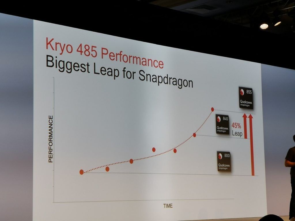
The latest ARM A76 architecture licensed for the Kryo 485 is another great contributor to the substantial year-on-year improvements we see with the Qualcomm Snapdragon 855. The A76 core is a brand new, blank slate design from ARM's Austin offices, featuring a new micro-architecture built from scratch to deliver what ARM calls "laptop-class performance with mobile efficiency." It is still a semi-custom design, and Qualcomm have made improvements such as optimized data pre-fetching for better efficiency, and a larger out-of-order execution window. This new design offers some tremendous performance improvements over the A75, which the Snapdragon 845's Gold cores were based on: it promises a 35% performance improvement, and 40% better power efficiency. When comparing the A75 on a 10nm process versus the A76 on a 7nm process at the same power envelope of 750mW/core, the performance advantage grows to 40% in the new core's favor, and energy savings can also climb to 50%. What's more, other improvements in Asymmetric Single Instruction Multiple Data (ASIMD) pipelines and dot-product instructions aggregate to ~3.9x improvements in the performance of machine learning tasks, like inference in convolutional neural networks. All of this amounts to industry-leading performance-per-area and a great complement to the new 7nm process, with Qualcomm's 2.84GHz 'Prime core' creeping close to the 3GHz reference clock speeds ARM had used when detailing the new core. All in all, Qualcomm promises an absolutely massive 45% CPU performance improvement over the 845, the largest year-on-year uplift yet.
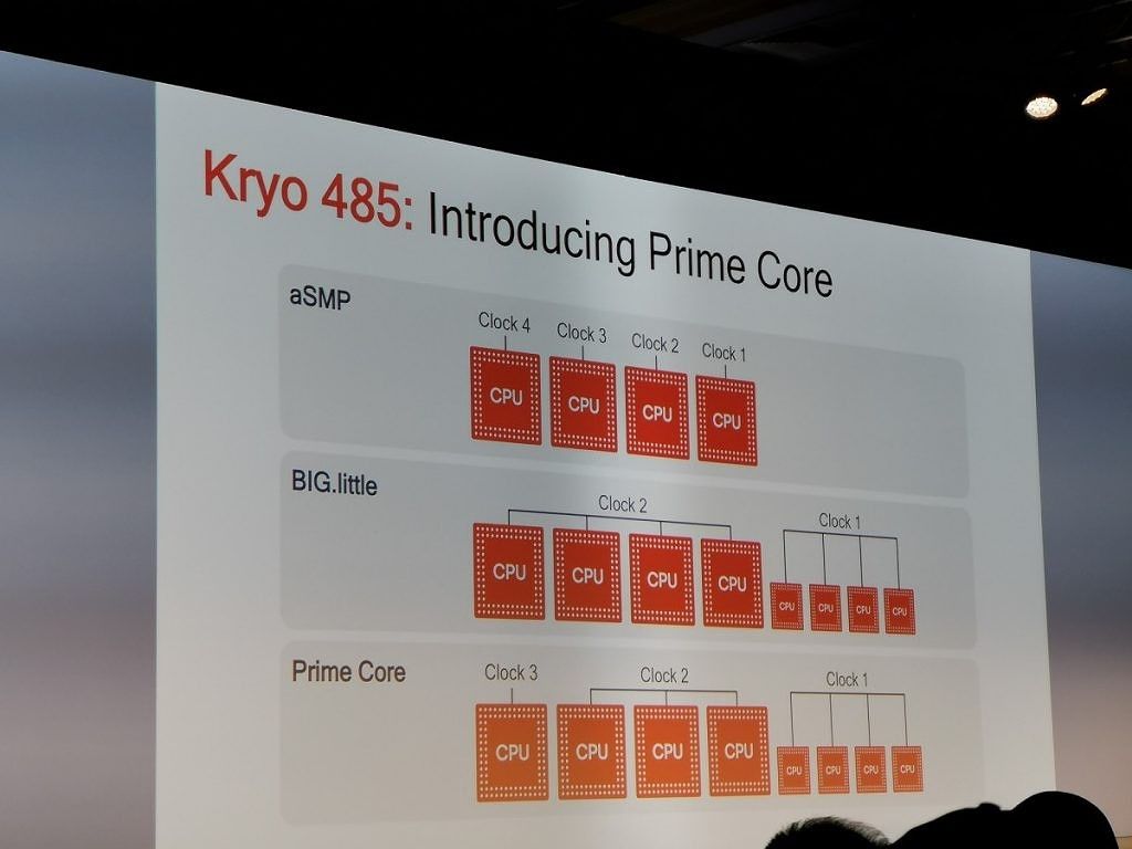
Speaking of the Snapdragon 855's 'Prime core', it's also not surprising to see Qualcomm move in with this new cluster setup given the improvements over big.LITTLE enabled by ARM's DynamIQ technology platforms. In essence, DynamIQ allows for more flexibility and scalability in multi-core processor design, allowing for multiple core designs in a given cluster, as well as fine-grained per core voltage control. (EDIT: In a Q&A, Qualcomm confirmed the Prime core shares its power domain with the performance cluster, limiting the utility described here). The A76 is a particularly good fit for such a lone premium core with its own clock, given it pushes the envelope when it comes to single-thread performance with 25% more integer instructions-per-clock than the A75, and 35% higher ASIMD and floating point performance, while offering 90% higher memory bandwidth. In short, the A76 presents a greater generational uplift than previous generations, which no doubt contributed to Qualcomm’s also greater-than-usual year-on-year performance bump for the Snapdragon 855 (for reference, Qualcomm cited 25 to 30% uplift for the 845 over the 835). This might be enough to put the Qualcomm Snapdragon 855's resulting performance ahead of Samsung LSI's Mongoose 3 (M3) core found in the Exynos 9810, though that particular design suffered from power efficiency in a way that Qualcomm chips have not, and that the Snapdragon 855 most likely will not either.
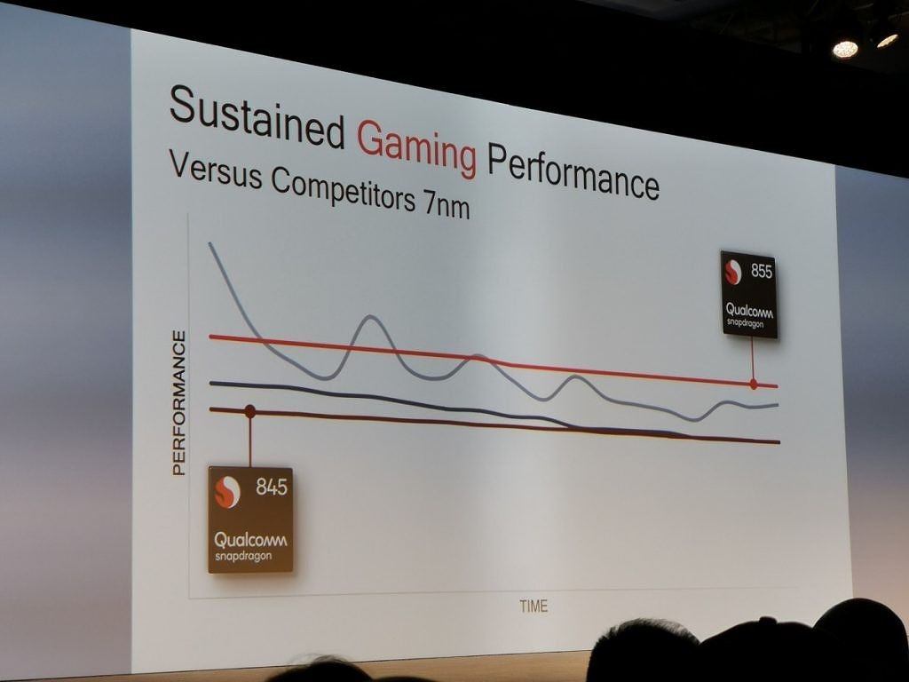
What does it mean for the end-user? Of course, we should expect increased benchmark cores—ARM projects 28% higher Geekbench scores for mobile, and 35% improved Javascript performance. Beyond benchmarks, which might bear little relation to the end-user experience, the A76 continues the A75's focus on sustained performance, meaning users should expect less throttling during prolonged gaming sessions. The move to 7nm combined with the new core design will most definitely result in noticeable battery life improvements for end users, and that's perhaps the most appealing feature of this set of upgrades. The new 'Prime' core is also interesting, given that a lone core focusing on top single-threaded performance could prove beneficial throughout applications and processes that aren't set up to take proper advantage of multi-threading. Of course, the 7nm manufacturing process further impacts other blocks of the Snapdragon 855 as well, carrying the same power savings to other compute units that are also involved in the day-to-day user experience, such as image processing for smartphone photography.
'Snapdragon Elite Gaming Experience' and Adreno 640 GPU
The Qualcomm Snapdragon 855 heavily focuses on gaming this time around, an unsurprising turn of events given the popularity of titles like Fortnite and PlayerUnknown’s Battlegrounds as well as the increasing popularity of mobile eSports (yes, this is a thing) in Asia. According to figures shown by Qualcomm from the Newzoo 2017 Global Games Market report, mobile gaming is trending up with an expected 2018 total revenue of $70.3 billion, constituting 51% of all gaming revenue thanks to a 25.5% year-on-year increase.
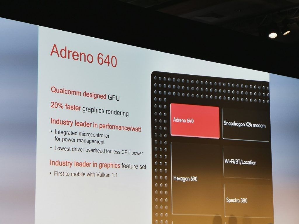
The Adreno 640 GPU brings a healthy 20% boost to graphics performance, further adding to Qualcomm’s lead over the competition in this particular area. For reference, though, the Snapdragon 845 brought a 30% uplift over the Snapdragon 835, which itself offered a 30% improvement over the Snapdragon 821 as well. Still, this should keep Qualcomm ahead in graphics performance, and most importantly, performance per watt if they manage to improve on that front as well. Beyond that figure, Qualcomm is as secretive as ever when it comes to the Adreno: we heard about the integrated micro-controller for power management, and how the 640 has the lowest driver overhead, though the company did mention the inclusion of 50% more arithmetic logic units (ALUs) that would further accelerate AI performance.
One thing Qualcomm spent a lot of time talking about on briefings is their desire to bring ‘physically-based rendering’ (PBR) to more mobile gaming experiences. PBR is a shading model that allows for realistic graphics rendering, accurately modeling light flow in accordance with the material represented in textures or the tessellation of the surface. This allows for in-game objects to properly mimic the visual properties of real-world materials, including the proper rendering of micro-surfaces like abrasions and specular highlights. The most noticeable improvements, though, come in how it allows a more accurate portrayal of the reflectivity and gloss of all surfaces, even those from flat and opaque (simulated) materials.
Qualcomm and the developers behind the popular Unity Engine have been working on making PBR more accessible, but the company also works with other engine and game developers in optimizing mobile games for Snapdragon devices. Game engines like Unity, Unreal, Messiah, and NeoX are already optimized for Snapdragon devices, for example, and the Snapdragon 855 supports the latest graphics APIs such as the new Vulkan 1.1. Studios like NetMarble, who is behind Lineage II: Revolutions, have also worked with Qualcomm in the past to best showcase the strengths of the Snapdragon platform. Moreover, with the Snapdragon 675, we saw talks of a custom algorithm that achieved up to 90% fewer janks compared to the same platform sans the optimizations, and the same changes have made their way to the Snapdragon 855. It still isn’t clear what these optimizations entail, and we don’t expect them to be applicable in every game, but it will most definitely mean better performance in, at least, the bigger titles on Android.
On top of all that, while the Snapdragon 835 and 845 allowed playback and capture (respectively) of 10-bit, true HDR video, the Qualcomm Snapdragon 855 will be the first mobile chipset that allows for true HDR gaming. This will necessitate true HDR-capable displays, which are luckily increasingly common among flagships smartphones. Because of this, users can expect richer colors with more tonal depth, higher dynamic range (as implied by the name), and improved contrast. This isn’t necessarily a must-have feature, but it’s certainly nice to have given that current HDR gaming setups require expensive HDR-ready TVs and monitors, as well as capable computers and specific gaming consoles. With the Qualcomm Snapdragon 855, HDR in gaming will arguably be more accessible and convenient (sans the touchscreen controls, of course).
A new Hexagon 690 DSP for AI workloads
While the company isn’t explicitly calling it a “neural processing unit” in its marketing materials, AI workloads will also benefit from the new-and-improved Hexagon 690 DSP. Qualcomm quietly introduced these co-processors many generations ago (with the proper introduction of the QDSP6 v6 alongside the 820), but it wasn’t until recently that they began pitching them as some of the better SoC blocks for AI. Originally designed for accelerating imaging workloads, the architecture of the DSP—in particular with the inclusion of Hexagon Vector eXtensions (HVX)—became a great fit for ML tasks. The DSP is more programmable than fixed-function hardware, while still retaining some of the performance and efficiency benefits that characterize application-specific processor blocks, greatly accelerating scalar and vector operations. This proved excellent for the ever-changing image processing algorithms that can be offloaded to the DSP, but also naturally lend itself to AI workloads. The Hexagon DSP has been a boon for machine learning on edge devices due to its excellent hardware-level multi-threading and parallel computing, capable of handling thousands of bits of vector units per processing cycle, compared to an average CPU core’s hundreds of bits per cycle, and servicing multiple offload sessions.
The Hexagon DSP is particularly well-suited for imaging tasks as it can stream data directly from the imaging sensor to the DSP’s local memory (L2 Cache), bypassing the device’s DDR memory controller. Google, for instance, used the Hexagon DSP’s image-processing to power the Pixel and Pixel 2’s HDR+ algorithms, before introducing their own Pixel Visual Core. It’s also Hexagon-ready devices that see the best results from the popular Google Camera ports, which you can explore here. It’s been used in virtual and augmented reality workloads, famously powering the now-defunct Project Tango on the Lenovo Phab 2 Pro and ASUS ZenFone AR. That said, most OEMs implementing Snapdragon flagship devices utilize the Hexagon DSP for image processing in one way or another, which you can verify using tools like Snapdragon Profiler.
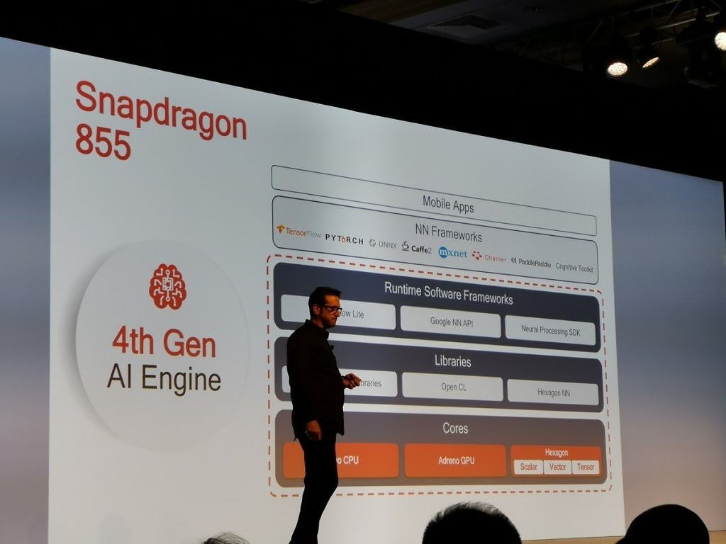
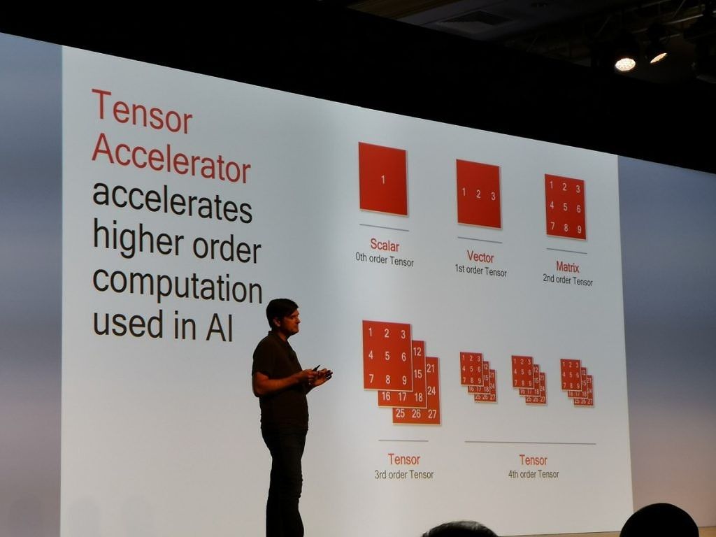
So what’s new with the new DSP? The Hexagon 690 doubled the number of vector accelerators (HVX) from two to four to work in tandem with the four scalar threads, which see improved performance of 20% as well. On top of that, the Hexagon 690 brings the first tensor accelerator for mobile with the Hexagon Tensor Accelerator (HTA). This is a significant addition: it serves as hardware acceleration for expensive matrix multiplication, and also integrates non-linearity functions (like sigmoid and ReLU) at the hardware level, further speeding up inference. These changes to the DSP should translate into better voice assistant performance, from hot-word detection to on-device command parsing, offering improved echo cancellation and noise suppression, for example. Qualcomm stresses that they provide a complete heterogeneous compute platform that allows AI workload to tap into either the CPU, GPU or DSP, or any combination of the three blocks -- in the words of Qualcomm's Gary Brotman, this it's "more than one core, it's more than hardware, it's a complete system". Their 4th-generation "Qualcomm AI Engine" goes beyond hardware too, as we also find support for the Snapdragon Neural Processing SDK and Hexagon NN to access the aforementioned blocks, as well as the Android NN API, and popular ML frameworks such as Caffe/Caffe 2, TensorFlow/Lite, and ONNX (Open Neural Network Exchange). In aggregate, the Snapdragon 855 can offer three times the raw AI performance of its predecessor (and twice compared to Huawei) , topping over 7 trillion operations per second (TOPs). Keep in mind, however, that Qualcomm continues to focus on a heterogeneous computing solution over focusing on a single dedicated block.
To learn more about the Hexagon DSP, check out last year’s piece detailing how it helps with AI workloads.
In summary, the compute package of the Snapdragon 855 brings some of the more impactful year-on-year improvements we’ve seen in recent years. The Spectra 380 ISP-CV, which we covered in a separate article, also brings tremendous boosts to performance and power efficiency, enabling excellent new features like 4K 60FPS HDR video recording with portrait mode or background swap (quite the flex!).
As explained in this article, these advancements and new features should tangibly made themselves felt throughout the user experience. We are looking forward to the Qualcomm Snapdragon 855 and getting to test it in-depth soon, so stay tuned to XDA-Developers for the latest Snapdragon 855 news and analysis!


